Hardware User Manual
Safety Instructions
|
|
Operating Environment
|
|
Mounting the Product
|
|
Using the Product
|
|
Power Supply
|
|
|
Electromagnetic and Electrostatic Interference Prevention
|
|
|
|
Laser Safety
|
Functional Diagrams
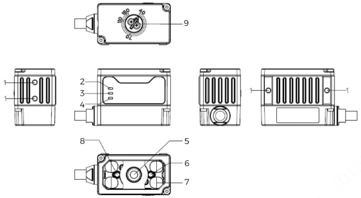
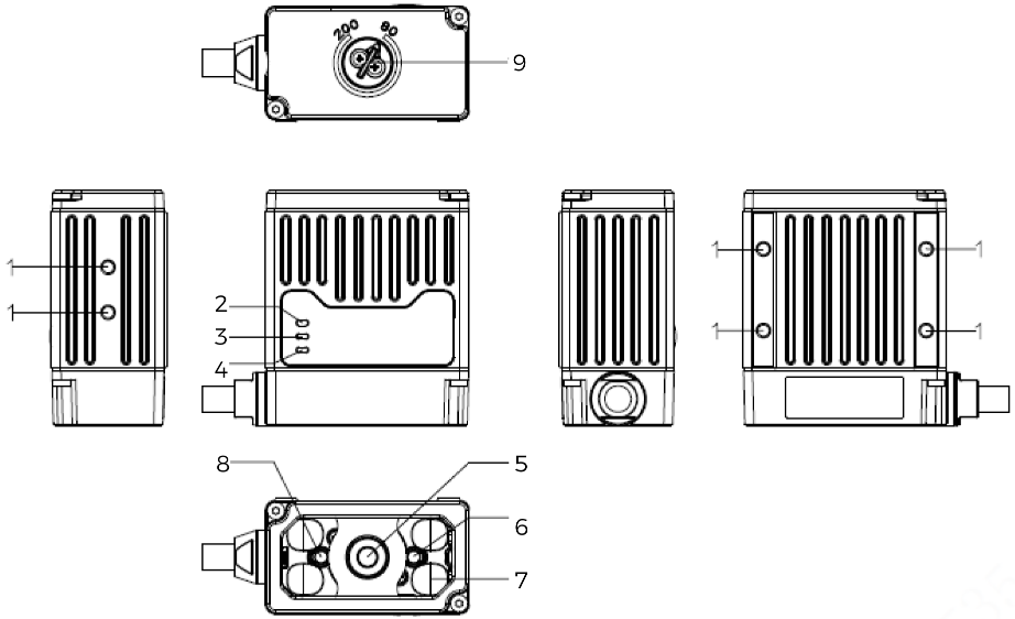
AIC-Lite-016M-07M-W-GL and AIC-Lite-016M-16M-W-GL
|
|
|
|
No. |
Name |
Function |
|---|---|---|
① |
Mounting hole |
Used to secure the camera, you can use the M3 screws provided in the box. |
② |
LINK indicator |
Network connection indicator Green solid on: network normal |
③ |
POWER indicator |
Power indicator Solid on: power normal Off: power abnormal |
④ |
OK/NG indicator |
Green: image captured successfully. |
⑤ |
Image sensor |
Used to capture image data. |
⑥ |
Orange dot indicator |
Can be turned on manually, used to assist in locating the workpiece under inspection. |
⑦ |
Fill light |
LED light source, provides fill lighting during image acquisition to ensure imaging quality. White light on the upper and lower sides, each can be set to high-frequency strobe, strobe or off. |
⑧ |
Green dot indicator |
Can be turned on manually, used to assist in locating the workpiece under inspection. |
⑨ |
Focus adjustment nut |
Adjust the focal length with the focus wrench to obtain clear images, ensuring image acquisition quality. |
AIC-Lite-050M-08A-W-GL and AIC-Lite-050M-16A-W-GL
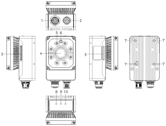
No. |
Name |
Function |
|---|---|---|
① |
Network interface |
Gigabit Ethernet interface, M12-A female socket, 8 pins. |
② |
Power and I/O interface |
Integrated power and trigger I/O, M12-A aviation male plug, 12 pins. |
③ |
Side indicator light |
Solid on: image captured successfully |
④ |
Image sensor |
Used to capture image data. |
⑤ |
Fill light |
LED light source, provides fill lighting during image acquisition to ensure imaging quality. Four independent channels, each can be set to steady on, strobe or off. |
⑥ |
Aimer |
Used for positioning. |
⑦ |
Mounting hole |
Used to secure the camera, you can use the M3 screws provided in the box. |
⑧ |
POWER indicator |
Power indicator Solid on: power normal Off: power abnormal |
⑨ |
LINK indicator |
Network connection indicator Solid on: network connection normal Flashing: data being transmitted Off: network connection abnormal |
⑩ |
STATUS indicator |
Solid on: the image sensor is in a triggered state and is acquiring image data Off: the camera is not currently acquiring data |
AIC-Lite-050C-08A-W-GL
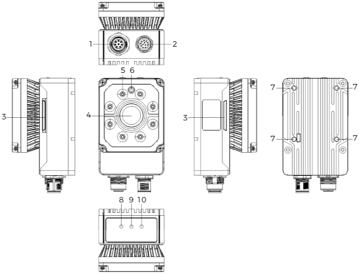
No. |
Name |
Function |
|---|---|---|
① |
Network interface |
Gigabit Ethernet interface, M12-A female socket, 8 pins. |
② |
Power and I/O interface |
Integrated power and trigger I/O, M12-A aviation male plug, 12 pins. |
③ |
OK/NG indicator |
Green: image captured successfully. |
④ |
Image sensor |
Used to capture image data. |
⑤ |
Fill light |
Polarized/non-polarized fill light, supports turning on or off. |
⑥ |
Aimer |
Used for positioning. |
⑦ |
Mounting hole |
Used to secure the camera, you can use the M3 screws provided in the box. |
⑧ |
POWER indicator |
Power indicator Solid on: power normal Off: power abnormal |
⑨ |
LINK indicator |
Network connection indicator Solid on: network connection normal Flashing: data being transmitted Off: network connection abnormal |
⑩ |
STATUS indicator |
Solid on: the image sensor is in a triggered state and is acquiring image data Off: the camera is not currently acquiring data |
AIC-Lite-120M-00C-N-GL, AIC-Lite-200M-00C-N-GL, and AIC-Lite-250M-00C-N-GL
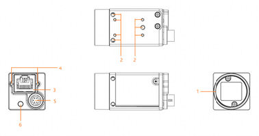
No. |
Name |
Function |
|---|---|---|
① |
Lens mount |
Used to install the lens. Please refer to the technical specifications to confirm the lens mount specifications for each model. |
② |
Mounting screw holes |
Used to secure the camera. Please refer to the technical specifications to confirm the mounting hole positions and applicable screw specifications for each model. |
③ |
Network interface |
Gigabit Ethernet interface, RJ45 port, used for data transmission. |
④ |
Ethernet port locking screw hole (M2) |
Used to secure the network cable connected to the camera, to avoid image acquisition anomalies caused by a loose connector. |
⑤ |
Power and I/O interface |
Integrates power, trigger I/O and serial communication, M6 connector, 6 pins. |
⑥ |
Indicator lights |
Used to display the camera operating status, please see the table below for details. |
Status |
Indicator status |
Description |
|
|---|---|---|---|
Normal status |
Red |
Red light fast flashing |
Device starting up. |
Blue |
Blue light low brightness |
IP assigned, application software API not connected to the device. |
|
Red and blue high brightness |
Application software API connected to the device, free mode, no image transmission. |
||
Blue light fast flashing |
Application software API connected to the device, free mode, image transmission active. |
||
Blue light slow flashing |
Trigger mode in use. |
||
Red/Blue |
Red and blue flashing alternately |
Firmware upgrading. |
|
Abnormal status |
Red |
Red light solid on |
Device abnormal (e.g., no data stream, firmware upgrade failure, etc.). |
Red light slow flashing |
Network disconnected. |
||
Power and Ethernet Electrical Specifications
AIC-Lite-016M-07M-W-GL and AIC-Lite-016M-16M-W-GL
Parameter |
Description |
|---|---|
Camera power specifications |
DC +9V to +26V, ripple < 1%, powered via the camera 12-pin M12 connector. |
Data output interface |
Fast Ethernet |
Input/Output interface |
1 opto-isolated input 1 opto-isolated output 1 GPIO (configurable as input or output) |
|
AIC-Lite-050M-08A-W-GL, AIC-Lite-050M-16A-W-GL, and AIC-Lite-050C-08A-W-GL
Parameter |
Description |
|---|---|
Camera power specifications |
DC +9V to +26V, ripple < 1%, powered via the camera 12-pin M12 connector. Cable wire gauge no less than 24 AWG. |
Data output interface |
Gigabit Ethernet |
Input/Output interface |
2 opto-isolated inputs (LINE0 to LINE1) 3 opto-isolated outputs (LINE2 to LINE4) |
|
The power supply must meet SELV and LPS requirements. |
I/O Electrical Specifications
AIC-Lite-016M-07M-W-GL and AIC-Lite-016M-16M-W-GL
Optocoupler-isolated input
Input voltage |
Description |
|---|---|
+26 VDC |
Maximum input voltage. Exceeding this voltage may damage the device. |
+0 to +24 VDC |
Safe operating input voltage range for I/O. |
+0 to +6 VDC |
Logic 0. |
+6 to +9 VDC |
Input switching threshold region; logic state is indeterminate. |
>+9 VDC |
Logic 1. |
The typical circuit of the optocoupler-isolated input is shown in the following figure.
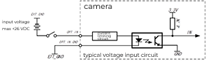
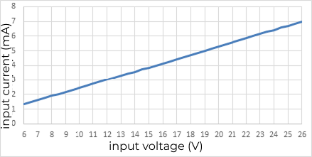
The relationship between sink current at the optocoupler-isolated input port and input voltage is shown in the following figure.
|
The relationship between input signal amplitude and trigger delay is shown in the following table.
Input signal amplitude (Vp-p) |
Rising-edge trigger delay tDR (µs) |
Falling-edge trigger delay tDF (µs) |
|---|---|---|
9 |
18.80 |
23.70 |
12 |
7.20 |
31.30 |
20 |
3.00 |
38.40 |
24 |
2.40 |
40.10 |
26 |
2.20 |
41.40 |
|
The trigger input delay measures the latency from the external optocoupler-isolated input port to the FPGA input pin, excluding the FPGA internal logic delay. |
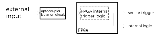
The minimum input pulse width requirement for the trigger input signal is shown in the following table.
Input signal amplitude (Vp-p) |
Minimum positive pulse width (µs) |
Minimum negative pulse width (µs) |
|---|---|---|
9 |
36.00 |
90.00 |
12 |
10.10 |
90.00 |
20 |
3.10 |
90.00 |
24 |
2.40 |
90.00 |
26 |
2.10 |
90.00 |
Optocoupler-Isolated Output
Voltage |
Description |
|---|---|
+26 VDC |
Maximum input voltage. Exceeding this voltage may damage the device. |
< +3.3 VDC |
I/O output may be abnormal. |
+3.3 to +24 VDC |
Safe operating range for I/O output. |
The typical circuit of the optocoupler-isolated output is shown in the following figure.
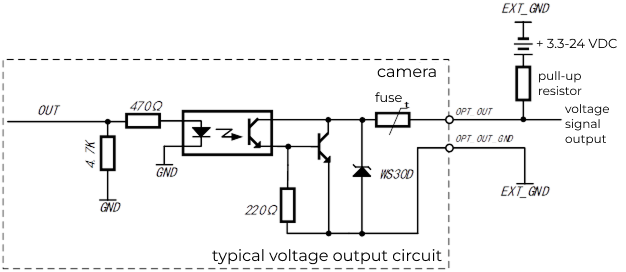
With a 1 kΩ pull-up resistor, the output rise/fall times and rising/falling edge delay times under different external supply voltages are as shown in the following table.
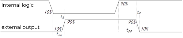
External supply voltage (V) |
Rise time tR (µs) |
Fall time tF (µs) |
Rising-edge trigger delay tDR (µs) |
Falling-edge trigger delay tDF (µs) |
|---|---|---|---|---|
5 |
19.70 |
3.20 |
39.9 |
8.06 |
12 |
24.06 |
5.22 |
44.8 |
11.8 |
24 |
30.11 |
8.10 |
44.8 |
53.2 |
|
The relationship between optocoupler-isolated output on-state voltage drop and output current is shown in the following figure.
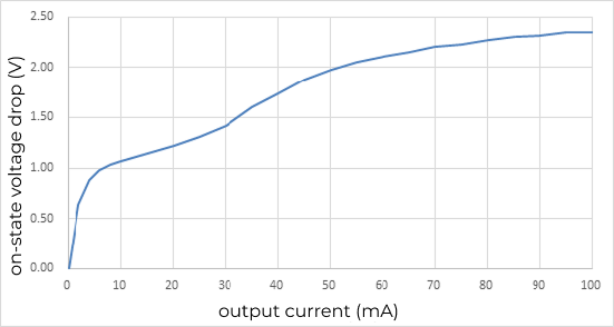
|
Configurable GPIO
GPIO as Input
Input voltage |
Description |
|---|---|
+26 VDC |
Maximum input voltage. Exceeding this voltage may damage the device. |
+0 to +24 VDC |
Safe operating input voltage range (minimum voltage is 3.3 VDC when externally pulled up) |
+0 to +0.8 VDC |
Logic 0. |
+0.8 to +2.2 VDC |
Input switching threshold region; logic state is indeterminate. |
>+2.2 VDC |
Logic 1. |
The typical circuit of the GPIO input is shown in the following figure.
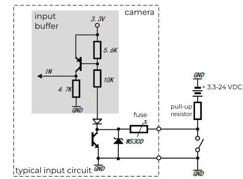
The relationship between GPIO input signal amplitude and trigger delay is shown in the following table:
Input signal amplitude (Vp-p) |
Rising-edge trigger delay tDR (µs) |
Falling-edge trigger delay tDF (µs) |
|---|---|---|
3.00 |
6.783 |
0.339 |
5.00 |
6.563 |
0.200 |
9.00 |
6.164 |
0.106 |
10.00 |
6.416 |
0.960 |
|
The relationship between sink current and external input voltage when GPIO is used as input is shown in the following figure.
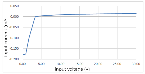
|
GPIO as Output
Voltage |
Description |
|---|---|
+26 VDC |
Maximum input voltage. Exceeding this voltage may damage the device. |
+3.3 to +24 VDC |
Safe operating voltage range during output. |
< +3.3 VDC |
I/O output may be abnormal. |
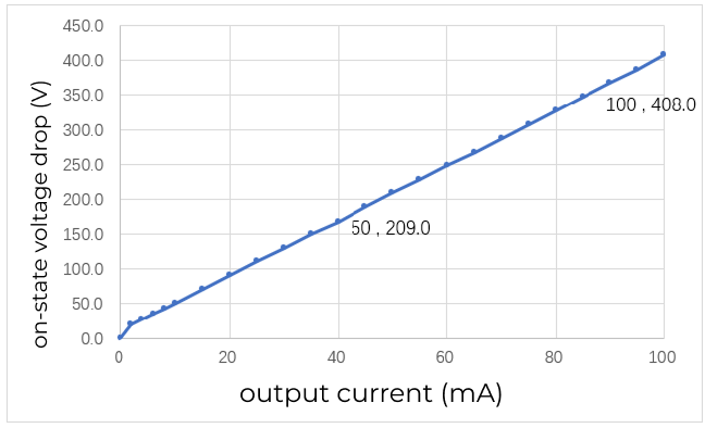
When GPIO is used as output, the maximum sink current is 50 mA. The typical circuit of the GPIO output is shown in the following figure.
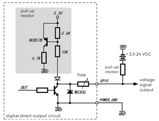
The relationship between the GPIO output on-state voltage drop (voltage drop between GPIO and GND) and output current (current flowing into the GPIO pin) is shown in the following figure.
|
The GPIO output signal delay diagram is shown in the following figure.
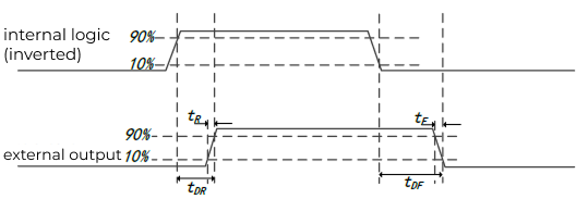
With a 470 Ω pull-up resistor, the output rise/fall times and rising/falling edge delay times under different external supply voltages are as shown in the following table.
External supply voltage (V) |
Rise time tR (µs) |
Fall time tF (µs) |
Rising-edge trigger delay tDR (µs) |
Falling-edge trigger delay tDF (µs) |
|---|---|---|---|---|
None |
- |
- |
5.43 |
0.35 |
5 |
0.16 |
0.02 |
1.80 |
39 |
12 |
0.22 |
0.04 |
2.37 |
71 |
|
AIC-Lite-050M-08A-W-GL, AIC-Lite-050M-16A-W-GL, and AIC-Lite-050C-08A-W-GL
Optocoupler-isolated input
Input voltage |
Description |
|---|---|
+26 VDC |
Maximum input voltage. Exceeding this voltage may damage the device. |
+0 to +24 VDC |
Safe operating input voltage range for I/O. |
+0 to +6 VDC |
Logic 0. |
+6 to +9 VDC |
Input switching threshold region; logic state is indeterminate. |
>+9 VDC |
Logic 1. |
The typical circuit of the optocoupler-isolated input is shown in the following figure.
The relationship between sink current at the optocoupler-isolated input port and input voltage is shown in the following figure.
|
The relationship between input signal amplitude and trigger delay is shown in the following table.
Input signal amplitude (Vp-p) |
Rising-edge trigger delay tDR (µs) |
Falling-edge trigger delay tDF (µs) |
|---|---|---|
9 |
18.80 |
23.70 |
12 |
7.20 |
31.30 |
20 |
3.00 |
38.40 |
24 |
2.40 |
40.10 |
26 |
2.20 |
41.40 |
|
The trigger input delay measures the latency from the external optocoupler-isolated input port to the FPGA input pin, excluding the FPGA internal logic delay. |
The minimum input pulse width requirement for the trigger input signal is shown in the following table.
Input signal amplitude (Vp-p) |
Minimum positive pulse width (µs) |
Minimum negative pulse width (µs) |
|---|---|---|
9 |
36.00 |
90.00 |
12 |
10.10 |
90.00 |
20 |
3.10 |
90.00 |
24 |
2.40 |
90.00 |
26 |
2.10 |
90.00 |
Optocoupler-Isolated Output
Voltage |
Description |
|---|---|
+26 VDC |
Maximum input voltage. Exceeding this voltage may damage the device. |
< +3.3 VDC |
I/O output may be abnormal. |
+3.3 to +24 VDC |
Safe operating range for I/O output. |
The typical circuit of the optocoupler-isolated output is shown in the following figure.
With a 1 kΩ pull-up resistor, the output rise/fall times and rising/falling edge delay times under different external supply voltages are as shown in the following table.
External supply voltage (V) |
Rise time tR (µs) |
Fall time tF (µs) |
Rising-edge trigger delay tDR (µs) |
Falling-edge trigger delay tDF (µs) |
|---|---|---|---|---|
5 |
19.70 |
3.20 |
39.9 |
8.06 |
12 |
24.06 |
5.22 |
44.8 |
11.8 |
24 |
30.11 |
8.10 |
44.8 |
53.2 |
|
The relationship between optocoupler-isolated output on-state voltage drop and output current is shown in the following figure.
|
AIC-Lite-120M-00C-N-GL, AIC-Lite-200M-00C-N-GL, and AIC-Lite-250M-00C-N-GL
Opto-Isolated Input
Input voltage |
Description |
|---|---|
+26 VDC |
Maximum input voltage. Exceeding this voltage may cause device damage. |
+0 to +24 VDC |
Safe operating voltage range for I/O input. |
+0 to +1.4 VDC |
Logic 0. |
+1.4 to +2.2 VDC |
Input switching threshold range; logic state is indeterminate. |
>+2.2 VDC |
Logic 1. |
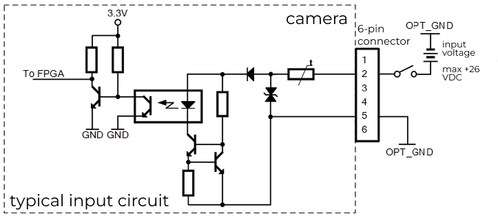
The typical circuit of the opto-isolated input is shown below.
|
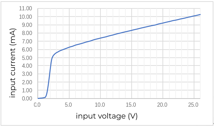
The relationship between input current and input voltage at the opto-isolated input port is shown below.
|
The above values are typical measurements at an ambient temperature of 25°C; individual differences exist between cameras. |
The relationship between input signal amplitude and delay for the opto-isolated input interface is shown in the table below:
Input signal amplitude (Vp-p) |
Rising-edge trigger delay tDR (µs) |
Falling-edge trigger delay tDF (µs) |
|---|---|---|
3.3 |
3.99 |
20.80 |
5 |
3.80 |
21.16 |
9 |
3.61 |
21.47 |
12 |
3.19 |
21.47 |
|
|
Opto-isolated output
Input voltage |
Description |
|---|---|
+26 VDC |
Maximum input voltage. Exceeding this voltage may cause device damage. |
+3.3 to +24 VDC |
Safe operating voltage range for I/O output. |
< +3.3 VDC |
I/O output may be abnormal. |
The typical circuit of the opto-isolated output is shown below.
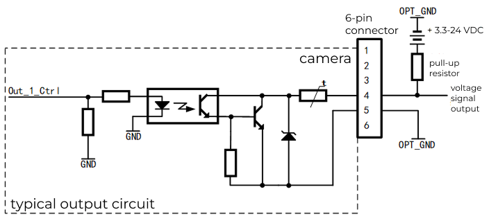
Output Delay vs. External Power Supply Voltage
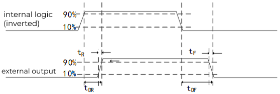
In some applications a pull-up resistor to an external supply is required to produce a high-level output. The pull-up resistor value depends on the external device and application scenario, but must not exceed the maximum allowable current of the opto-isolated output port. The larger the pull-up resistor value, the smaller the optocoupler conduction voltage drop; the longer the output waveform rise/fall time; and the smaller the external drive capability. The maximum current of the opto-isolated output is 50 mA, and the timing diagram of the opto-isolated output signal delay is shown below.
|
Recommended pull-up resistor values under different external supply voltages are as follows: 1 kΩ for 3.3 V or 5 V supply; 2.4 kΩ for 12 V supply; 4.7 kΩ for 24 V supply. |
When using a 1 kΩ pull-up resistor, the output rise/fall time and rising/falling edge delay time under different external supply voltages are shown in the table below.
External supply voltage (V) |
Rise time tR (µs) |
Fall time tF (µs) |
Rising-edge trigger delay tDR (µs) |
Falling-edge trigger delay tDF (µs) |
|---|---|---|---|---|
5 |
19.70 |
3.20 |
39.9 |
8.06 |
12 |
24.06 |
5.22 |
44.8 |
11.8 |
24 |
30.11 |
8.10 |
44.8 |
53.2 |
|
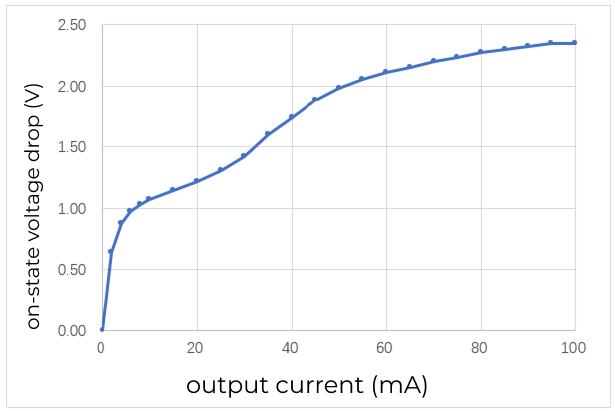
Output Conduction Voltage Drop vs. Output Current
The relationship between opto-isolated output conduction voltage drop and output current is shown below.
|
Optocoupler Interface as Transistor Output
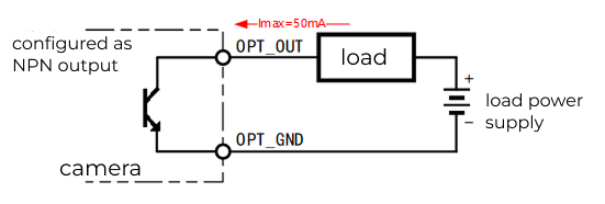
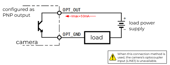
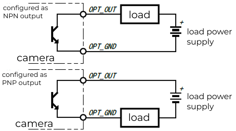
The camera’s transistor output is isolated from internal circuits via an optocoupler, therefore the transistor output can be used as NPN or PNP output. When used as PNP output, opto input LINE1 is not available. The connection methods for the opto interface as NPN output and as PNP output are shown below.
|
When using the camera’s opto output to connect a tungsten filament lamp load, avoid direct connection. A tungsten filament lamp generates an inrush current about 10 to 15 times the steady-state current at turn-on, which may exceed the maximum allowable current of the opto-isolated output, leading to damage to the output interface. It is recommended to isolate and protect it via a replaceable plug-in interposing relay or by adding an inrush current limiter in the circuit.
Configurable GPIO
GPIO as Input
Input voltage |
Description |
|---|---|
+26 VDC |
Maximum input voltage. Exceeding this voltage may damage the device. |
+0 to +24 VDC |
Safe operating input voltage range (minimum voltage is 3.3 VDC when externally pulled up) |
+0 to +0.8 VDC |
Logic 0. |
+0.8 to +2.2 VDC |
Input switching threshold region; logic state is indeterminate. |
>+2.2 VDC |
Logic 1. |
The relationship between GPIO input signal amplitude and trigger delay is shown in the following table:
Input signal amplitude (Vp-p) |
Rising-edge trigger delay tDR (µs) |
Falling-edge trigger delay tDF (µs) |
|---|---|---|
3.00 |
6.783 |
0.339 |
5.00 |
6.563 |
0.200 |
9.00 |
6.164 |
0.106 |
10.00 |
6.416 |
0.960 |
|
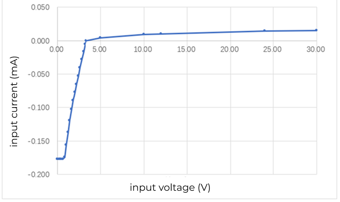
The relationship between sink current and external input voltage when GPIO is used as input is shown in the following figure.
|
GPIO as Output
Voltage |
Description |
|---|---|
+26 VDC |
Maximum input voltage. Exceeding this voltage may damage the device. |
+3.3 to +24 VDC |
Safe operating voltage range during output. |
< +3.3 VDC |
I/O output may be abnormal. |
When GPIO is used as output, the maximum sink current is 50 mA. The typical circuit of the GPIO output is shown in the following figure.
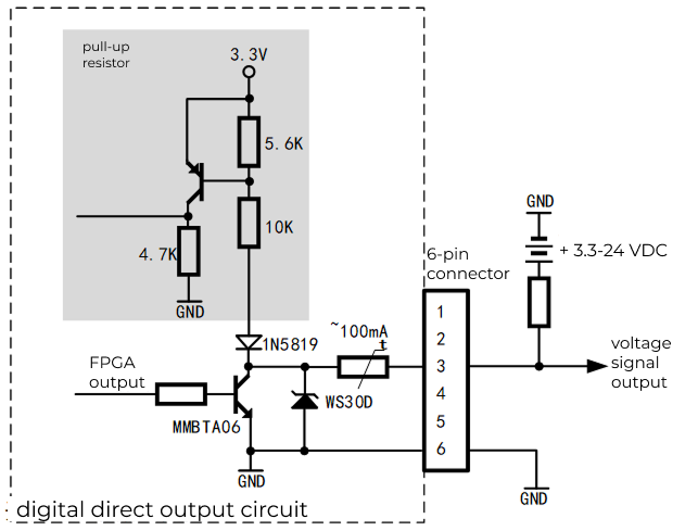
The relationship between the GPIO output on-state voltage drop (voltage drop between GPIO and GND) and output current (current flowing into the GPIO pin) is shown in the following figure.
|
The GPIO output signal delay diagram is shown in the following figure.
With a 470 Ω pull-up resistor, the output rise/fall times and rising/falling edge delay times under different external supply voltages are as shown in the following table.
External supply voltage (V) |
Rise time tR (µs) |
Fall time tF (µs) |
Rising-edge trigger delay tDR (µs) |
Falling-edge trigger delay tDF (µs) |
|---|---|---|---|---|
None |
- |
- |
5.43 |
0.35 |
5 |
0.16 |
0.02 |
1.80 |
39 |
12 |
0.22 |
0.04 |
2.37 |
71 |
|
Package Contents
Model |
Standard accessories |
Optional accessories |
|---|---|---|
AIC-Lite-016M-07M-W-GL and AIC-Lite-016M-16M-W-GL |
Camera |
Camera power and I/O cable (15m) |
Camera power and I/O cable (5m) |
Power adapter |
|
M3 Phillips countersunk screws |
AC power cable |
|
User manual |
Switching power supply |
|
- |
Switching power supply AC power cable |
|
- |
Mounting bracket |
|
AIC-Lite-050M-08A-W-GL, AIC-Lite-050M-16A-W-GL, and AIC-Lite-050C-08A-W-GL |
Camera |
Camera power and I/O cable (15m) |
Camera power and I/O cable (5m) |
Gigabit Ethernet cable (15m) |
|
Gigabit Ethernet cable (5m) |
Power adapter |
|
M4 Phillips countersunk screws |
AC power cable |
|
User manual |
Switching power supply |
|
- |
Switching power supply AC power cable |
|
- |
Mounting bracket |
|
AIC-Lite-120M-00C-N-GL, AIC-Lite-200M-00C-N-GL, and AIC-Lite-250M-00C-N-GL |
Camera |
Camera power and I/O cable (30m) |
Camera power and I/O cable (5m) |
Gigabit Ethernet cable (30m) |
|
Gigabit Ethernet cable (5m) |
Industrial camera lens |
|
M3 Phillips countersunk screws |
Power adapter |
|
User manual |
AC power cable |
|
- |
Switching power supply |
|
- |
Switching power supply AC power cable |
|
Camera Mounting
Mount through the Camera Bracket
-
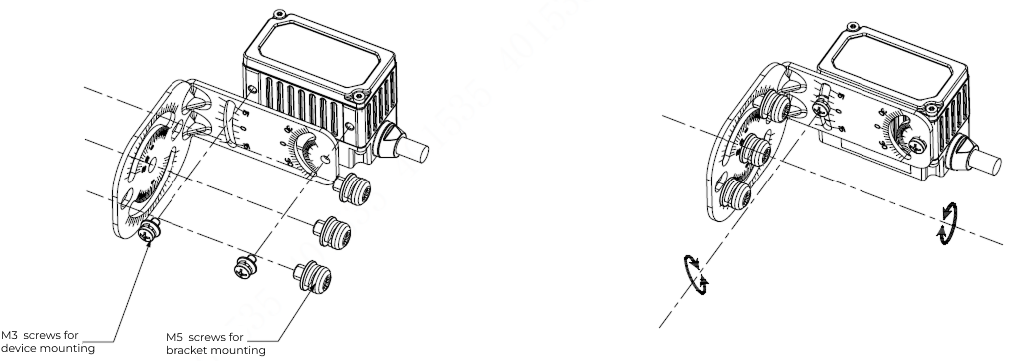
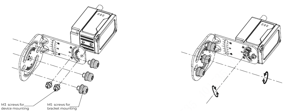
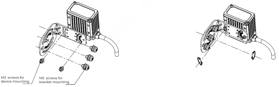
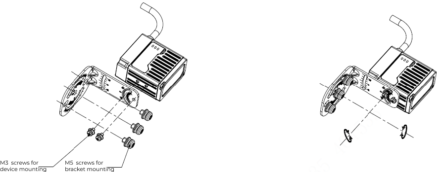
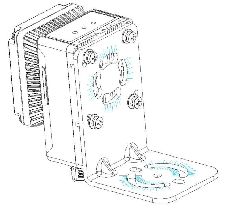
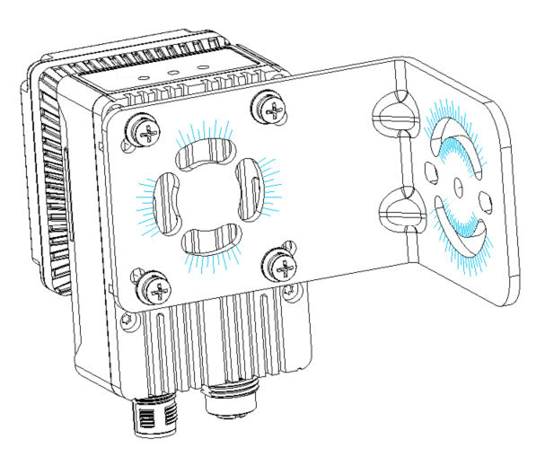
After confirming the mounting position, use M5 screws to fasten the mounting bracket to the mounting surface.
-
Insert screws of the corresponding specification into the mounting holes and tighten them to secure the camera to the mounting bracket.
-
AIC-Lite-016M-07M-W-GL and AIC-Lite-016M-16M-W-GL: M3 Phillips countersunk screws
-
AIC-Lite-050M-08A-W-GL, AIC-Lite-050M-16A-W-GL, andAIC-Lite-050C-08A-W-GL: M4 Phillips countersunk screws
-
|
AIC-Lite-120M-00C-N-GL, AIC-Lite-200M-00C-N-GL, and AIC-Lite-250M-00C-N-GL do not include a mounting bracket. Design a mounting bracket yourself if needed. |
-
AIC-Lite-016M-07M-W-GL (rear mounting):
-
AIC-Lite-016M-07M-W-GL (side mounting):
-
AIC-Lite-016M-16M-W-GL (rear mounting):
-
AIC-Lite-016M-16M-W-GL (side mounting):
-
AIC-Lite-050M-08A-W-GL, AIC-Lite-050M-16A-W-GL, and AIC-Lite-050C-08A-W-GL (rear mounting):
Mounting through Camera Threaded Holes
-
Open the camera’s lens cap or dust cap, and install a lens of the appropriate specification. If the lens mount is incompatible, use a corresponding lens adapter ring. AIC-Lite-016M-07M-W-GL, AIC-Lite-016M-16M-W-GL, AIC-Lite-050M-08A-W-GL, AIC-Lite-050M-16A-W-GL, and AIC-Lite-050C-08A-W-GL do not require a lens.
-
Insert screws of the corresponding specification into the mounting holes and tighten them to secure the camera to the mounting surface.
-
AIC-Lite-016M-07M-W-GL, AIC-Lite-016M-16M-W-GL, AIC-Lite-120M-00C-N-GL, AIC-Lite-200M-00C-N-GL, and AIC-Lite-250M-00C-N-GL: M3 Phillips countersunk screws
-
AIC-Lite-050M-08A-W-GL, AIC-Lite-050M-16A-W-GL, and AIC-Lite-050C-08A-W-GL: M4 Phillips countersunk screws
-
I/O External Wiring
AIC-Lite-016M-07M-W-GL, AIC-Lite-016M-16M-W-GL, AIC-Lite-050M-08A-W-GL, AIC-Lite-050M-16A-W-GL and AIC-Lite-050C-08A-W-GL
Opto-Isolated Input
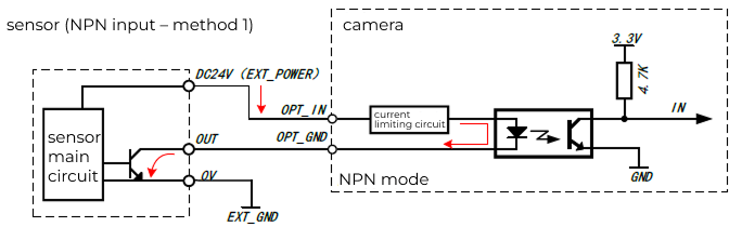
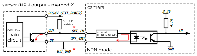
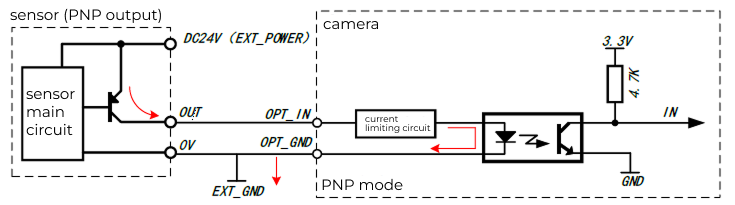
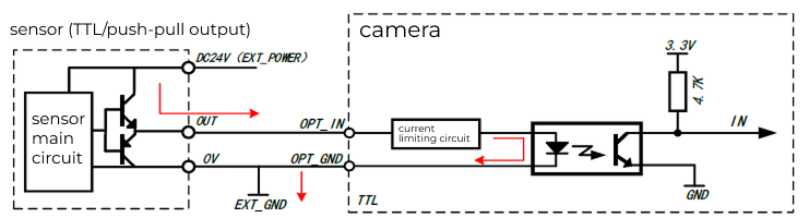
Opto-isolated inputs support sensors with NPN/PNP/push-pull output structures.
Sensors with NPN Output
-
Method 1: No pull-up resistor added (recommended).
-
Method 2: Add a pull-up resistor.
-
EXT_POWER refers to the positive terminal of the user’s external power supply, and EXT_GND refers to the ground of the user’s external power supply. The external power supply can be a standalone switching power supply or the sensor’s power supply.
-
This wiring method applies to sensors with NPN open-collector output structure.
-
Recommended pull-up resistor values: 1kΩ at 3.3V supply,1kΩ at 5V supply,2.4kΩ at 12V supply, 4.7kΩ at 24V supply. If higher output current capability is required, you may choose a resistor less than 1kΩ, but its rated power should be higher than 1W.
-
In some models, OPT_IN_GND and OPT_OUT_GND are shared, named OPT_GND.
-
Opto-Isolated Output
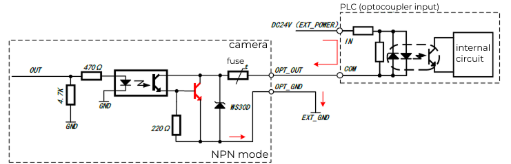
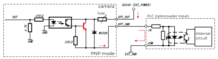
The camera’s transistor output is isolated from the internal circuitry by an optocoupler, so the transistor output can be used as NPN output or PNP output.
GPIO
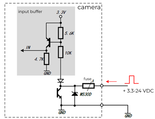
GPIO as Output
When GPIO is used as an output, its operation is similar to the opto-isolated output. However, GPIO uses non-isolated wiring, and the GPIO signal ground is common with the camera power ground.
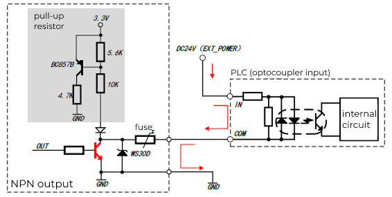
|
Wiring Method for Inductive Loads Such as Relays
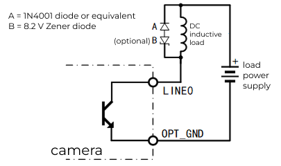
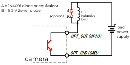
When using the camera output to drive inductive loads (such as relays), you must use relays with built-in flyback diodes or add an external flyback diode; otherwise, the output interface may be damaged by overvoltage.
The figure below shows an example of a DC inductive load suppression circuit. In most applications, using only the additional diode A is sufficient; if the application requires faster turn-off, it is recommended to also add the Zener diode B.Please ensure the selected Zener diode meets the current requirements of the output circuit.
AIC-Lite-120M-00C-N-GL, AIC-Lite-200M-00C-N-GL, and AIC-Lite-250M-00C-N-GL
Opto-Isolated Input
Sensors with NPN Output
-
Method 1: Add a pull-up resistor.
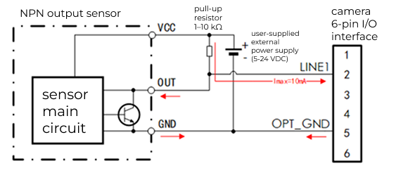
With this connection, the camera’s opto-isolated input LINE1 and opto-isolated output LINE0 can both be used.The schematic for connecting an NPN-output sensor to the opto-isolated input is shown below.
-
Recommended pull-up resistance: 1 to 10kΩ. In general,1kΩ at 5V supply, 2.4kΩ at 12V supply, 4.7kΩ at 24V supply.
-
The camera’s LINE1 input logic state is opposite to the sensor output state. When the sensor output is "ON", the internal transistor of the sensor is conducting, OUT and GND are shorted, LINE1 input is low level, corresponding to logic value "0"; when the sensor output is "OFF", the transistor is cut off, OUT is pulled to the external power supply voltage through the external pull-up resistor, LINE1 input is high level, corresponding to logic value "1".
-
The red arrows indicate the current direction (same below).
-
-
Method 2: No pull-up resistor added.
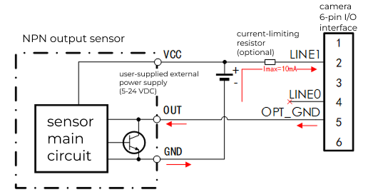
With this connection, only the camera’s opto-isolated input LINE1 is available, the opto-isolated output LINE0 is not available. The schematic for connecting an NPN-output sensor to the opto-isolated input is shown below.
-
In general, no series current-limiting resistor is required. When the external power supply is 24V and the supply voltage is unstable, it is recommended to insert a 1kΩ resistor in series at the LINE1 input to avoid overvoltage in the input circuit and damaging the camera.
-
The camera’s LINE1 input logic state matches the sensor output state. When the sensor output is "ON", the sensor’s internal transistor conducts, OUT and GND are shorted, external supply current flows through the current-limiting resistor (optional) into LINE1, then through the camera’s internal optocoupler input circuit, flows out from OPT_GND, and finally returns to the external power ground GND through the sensor’s internal transistor.
-
Sensors with PNP Output
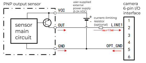
|
Sensors with TTL Output
With this connection, the camera’s opto-isolated input LINE1 and opto-isolated output LINE0 can both be used.The schematic for connecting a TTL circuit output to the opto-isolated input is shown below.
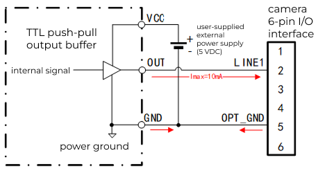
|
The TTL circuit can be a frame grabber or a sensor with complementary push-pull output. |
Application Examples of Connecting the Camera to a PLC
In transistor-type PLC output circuits, the I/O that sources current to the outside is called source (Source) output, and the I/O that sinks current is called sink (Sink) output.Sink outputs typically use NPN transistors, while source outputs typically use PNP or NPN transistors.Multiple PLC outputs share the same common terminal (COM), the common terminal of sink outputs connects to power ground (0V), and the common terminal of source outputs connects to the power supply (VCC).
-
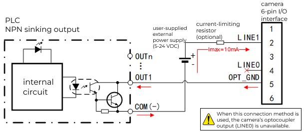
Connecting a PLC with sink (common collector) output
-
Method 1: No pull-up resistor added.
With this connection, only the camera’s opto-isolated input LINE1 is available,the opto-isolated output LINE0 is not available.The schematic for connecting the opto input to a PLC with sink output is shown below.
-
In the PLC-side output circuit shown above, Omron CP1E-E10 PLC is used as an example, where COM is the common terminal and OUT1 to OUTn are output terminals sharing the same common terminal.
-
With this connection, the camera’s opto-isolated output LINE0 is not available.
-
In general, no series current-limiting resistor is required. When the external power supply is 24V and the supply voltage is unstable, it is recommended to insert a 1kΩ resistor in series at the LINE1 input to avoid overvoltage in the input circuit and damaging the camera.
-
-
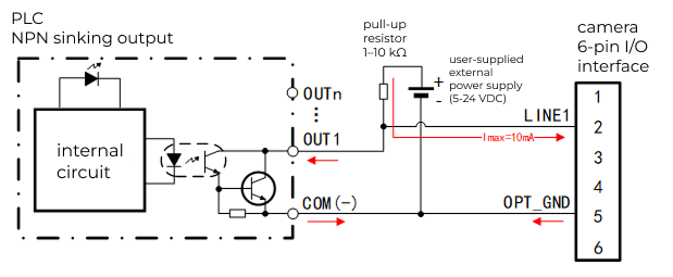
Method 2: Add a pull-up resistor.
With this connection, the camera’s opto-isolated input LINE1 and opto-isolated output LINE0 can both be used.The schematic for connecting the opto input to a PLC with sink output is shown below.
-
In the PLC-side output circuit shown above, Omron CP1E-E10 PLC is used as an example, where COM is the common terminal and OUT1 to OUTn are output terminals sharing the same common terminal.
-
Recommended pull-up resistance: 1 to 10kΩ. In general,1kΩ at 5V supply, 2.4kΩ at 12V supply, 4.7kΩ at 24V supply.
-
The camera’s input logic state is opposite to the PLC output state.
-
-
-
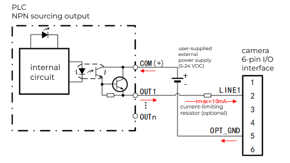
Connecting a PLC with source (common emitter) output
The schematic for connecting the opto input to a PLC with source output is shown below.
-
In the PLC-side output circuit shown above, Omron CP1E-E10 PLC is used as an example, where COM is the common terminal and OUT1 to OUTn are output terminals sharing the same common terminal.
-
In general, no series current-limiting resistor is required. When the external power supply is 24V and the supply voltage is unstable, it is recommended to insert a 1kΩ resistor in series at the LINE1 input to avoid overvoltage in the input circuit and damaging the camera.
-
The camera’s input logic state is the same as the PLC output state.
-
Opto-Isolated Output
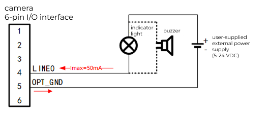
Optocoupler as NPN Output Connecting Indicator Light and Buzzer
The schematic for connecting an indicator light with the optocoupler as an NPN output is shown below.
|
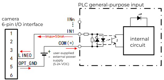
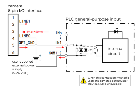
The red arrows indicate the current direction when the optocoupler output is conducting(logic "1")(same below). |
Optocoupler as NPN Output Connecting PLC Input
The schematic for connecting to PLC input with the optocoupler as an NPN output is shown below.
|
In the PLC-side output circuit shown above, Omron CP1E-E10 PLC is used as an example, where COM is the common terminal and IN1 to INn are input terminals sharing the same common terminal. |
Optocoupler as PNP Output Connecting PLC Input
The schematic for connecting to PLC input with the optocoupler as a PNP output is shown below.
|
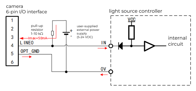
Optocoupler as NPN Output Connecting a Light Source Controller
Connecting a light source controller with the optocoupler as an NPN output is shown below.
|
Pull-up resistor value: 1 to 10kΩ,recommended value: 3.3V. In general,1kΩ at 5V supply, 2.4kΩ at 12V supply, 4.7kΩ at 24V supply. If the light source controller has a built-in pull-up resistor, an external pull-up resistor is not required. |
GPIO
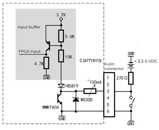
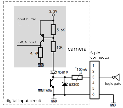
GPIO as Input
The schematic for connecting a mechanical switch with GPIO as input is shown below.
The schematic for connecting a 5V TTL logic output with GPIO as input is shown below.
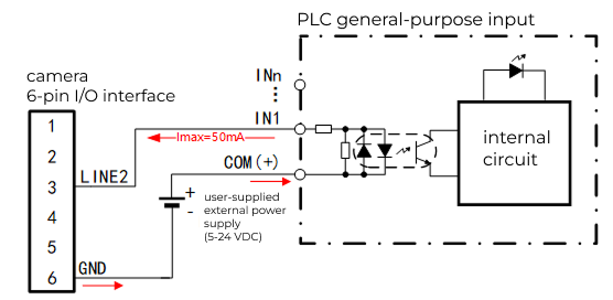
GPIO as Output
The schematic for connecting to PLC input with GPIO as output is shown below.
|
Maintenance
Regular Inspections
The camera is a precision instrument. Please perform the following inspections regularly to ensure the camera remains in optimal working condition.
Check External Conditions
| Inspection | Corrective actions | Recommended frequency |
|---|---|---|
Check for wear, scuffs, and deformation on the housing. |
Adjust the position or motion path of surrounding equipment to avoid friction or collision with the camera. |
Once per day |
Check for water stains or condensation inside the lens glass. |
Contact technical support or return to Mech-Mind for repair. |
Check Cables
| Inspection | Corrective actions | Recommended frequency |
|---|---|---|
Check whether the cable connections to the equipment are secure. |
Tighten cable connections. |
Once per day |
Check whether cables are bent or twisted. |
Improve routing to avoid excessive bending and twisting. The bend radius should be no less than 8 times the cable’s outer diameter (8D). |
|
Check whether cables are aged, worn, or damaged. |
Contact Mech-Mind to replace the cable. |
|
Check whether the cables have a burnt smell. |
Contact Mech-Mind to replace the cable, and investigate the location and cause of the burning to prevent recurrence. |
Cleaning
-
Clean the camera in a clean, enclosed indoor environment to avoid dust or particulate contamination. Be sure to disconnect the power before cleaning; otherwise, there may be a risk of electric shock.
-
If you need to remove the lens, first orient the camera’s imaging surface downward, then unscrew the lens, and immediately install the original lens cap or a dust cap before cleaning. If the camera will not be used after cleaning, ensure the lens cap is installed and place the camera with the imaging surface facing downward.
-
When cleaning the body, use a clean soft cloth to wipe away dust and debris. To remove stains on the window glass, use a clean, soft, lint-free cloth moistened with lens cleaner or glass cleaner to gently wipe, to avoid scratching the window glass. Daily cleaning is recommended.
-
We recommend using cleaning wipes or cleaners whose primary active ingredient is isopropyl alcohol. Do not use gasoline, kerosene, or other corrosive substances. These may damage the product’s exterior and internal structure. Do not use compressed air to accelerate drying, nor use pressure washers or hoses to spray rinse. Mech-Mind assumes no responsibility for damage caused by water ingress or improper cleaning.
-
Before reusing this product after long-term storage, please clean it first.
Storage
-
AIC-Lite-016M-07M-W-GL, AIC-Lite-016M-16M-W-GL, AIC-Lite-050M-08A-W-GL, AIC-Lite-050M-16A-W-GL, AIC-Lite-050C-08A-W-GL: The product protection rating is IP65. It effectively prevents dust from entering the interior and affecting its function. During use, avoid immersing the product in water for long periods, placing it in high-humidity environments, or leaving it outdoors for extended durations. When not in use, store it indoors in a cool, dry, and well-ventilated place. Product storage temperature range: -30 to 70°C.
-
AIC-Lite-120M-00C-N-GL, AIC-Lite-200M-00C-N-GL, and AIC-Lite-250M-00C-N-GL: The product protection rating is IP40. It can prevent solid foreign objects from entering the interior, but it is not waterproof. When not in use, store it indoors in a cool, dry, and well-ventilated place. Avoid environments that are persistently humid, dusty, extremely hot or cold, subject to strong electromagnetic radiation, or with unstable lighting conditions. Product storage temperature range: -30 to 80°C.
|
Disclaimer
It is strongly recommended to use the power supply and cables provided by Mech-Mind to ensure compliance with the safety and EMC standards. Mech-Mind shall not be liable for any issues caused by using the power supply and cables provided by a third party.
Trademark and Legal Statement
Mech-Mind and Mech-Mind series logos including  are registered trademarks of Mech-Mind Robotics Technologies Co., Ltd. and other related entities.
© Copyright 2026, Mech-Mind Robotics Technologies Co., Ltd.
Unless authorized in writing in advance by Mech-Mind Robotics Technologies Co., Ltd. (“Mech-Mind”), no part of the trademarks shall be used, reproduced, modified, transmitted, transcribed, or used or sold with other products as a bundle by any entity or individual in any form for any reason.
Any infringement of Mech-Mind’s trademark rights will be punished in accordance with the law.
Mech-Mind reserves all rights regarding this user manual. According to copyright laws, unless authorized by Mech-Mind, this user manual shall not be reproduced, modified, or issued in part or in its entirety by any entity or individual. Users who purchased and use the product may download, print, or copy the user manual for personal use or use inside the belonging organization. Unless authorized by Mech-Mind, the contents of the user manual may not be used for any other purposes.